Since we have a vinyl cutter at the Fort Collins Creator Hub and we all love electronic circuits of some sort (right?), why not try our hand at making a printed circuit on this cutting machine! It’s worth a try:
 Simple is good
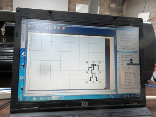
Here we have a very simple circuit. I used the free Eagle CAD software to make this particular one but I really could have easily made this one using MS-Paint. I won’t go into this part of the process… what we are really trying to do is see if we could actually make a PCB with a vinyl cutter – Because WE HAVE A VINYL CUTTER! The picture above shows the screen from the program called “Sure Cuts-A-Lot”. The PCB artwork was originally a “.PNG” file that was loaded into the Cuts-A-Lot program using the “Trace Image” feature of the program.
 Cutting the image in vinyl
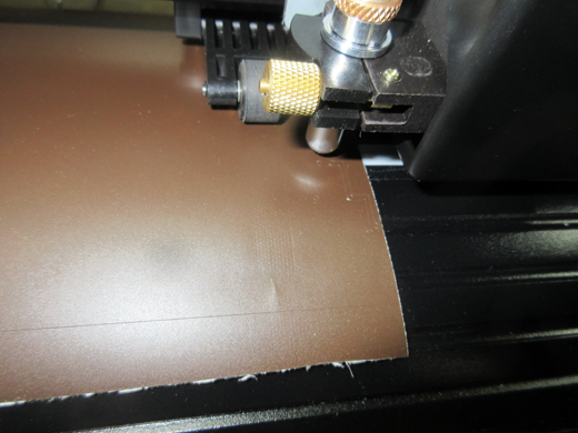
For this project, we are going to see how well the vinyl material works as an acid resist when its attached to a copper clad phenolic board.The vinyl should act as a mask while it is stuck to the copper. What we don’t know at this point is how well the glue on the vinyl will hold up to the acid etch. If the vinyl lifts up from the copper during the etching process, the circuit is ruined.
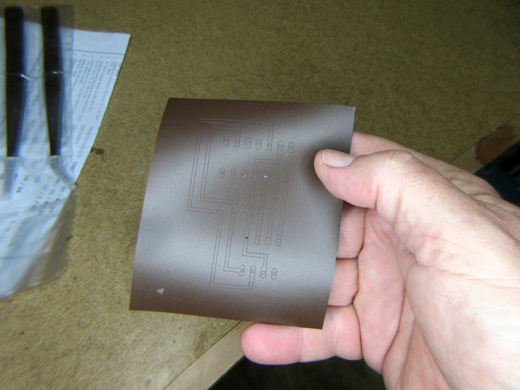
 A sample trace pattern cut on vinyl
The above picture shows a different circuit that was also used for testing. It this vinyl piece, the PCB holes are also cut into the pattern. The holes in the pattern seemed like a good idea, but they proved to be rather difficult to remove during the “weeding” process. Yes, weeding out those tiny pieces of vinyl is not worth the trouble; I’ll just figure out where the holes will go later.
 The vinyl after weeding
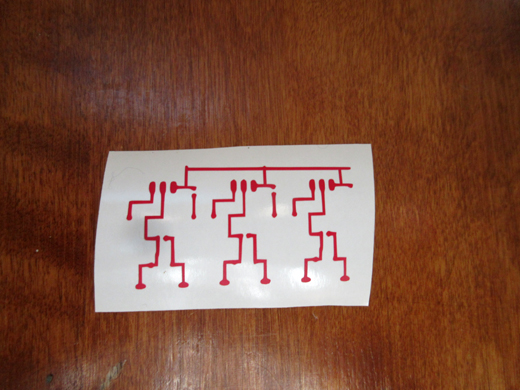
This is the vinyl “mask” that will adhere to the copper and act as an acid resist. Weeding out the larger pieces of vinyl while keeping the thin trace lines intact is not easy to do; I am not sure that I would want to try this using a more complicated circuit.
 Tape applied to the vinyl circuit
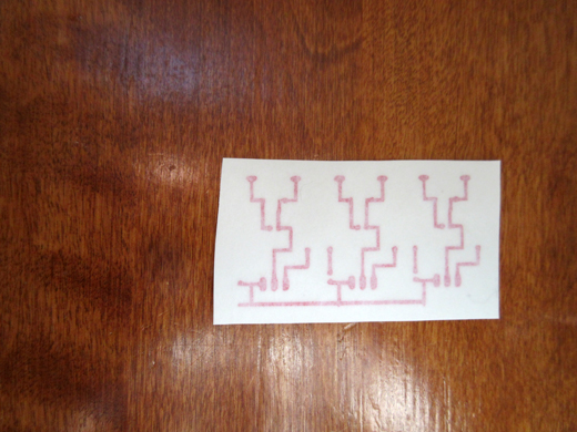
The vinyl cutting / pasting process requires a method for removing the image from the backing material before it can be applied to the substrate. Some care must be used when removing the tape; you want to make sure all of the vinyl traces adhere to the tape as you peel it off.
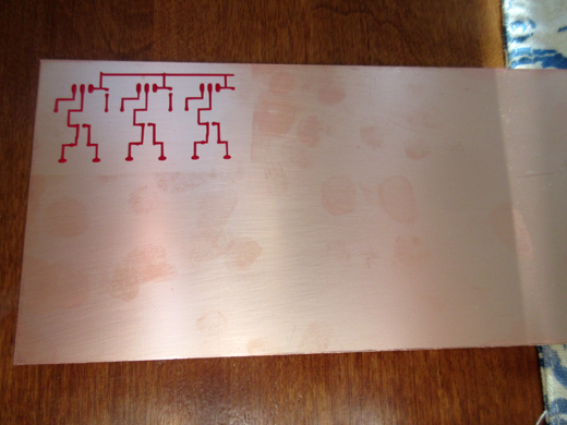
 The transfer to the copper
As it happens I have some sheets of copper clad PCB sheets ready for etching! Before the transfer, I removed the surface oxides with some fine steel wool and then I gave the board a final cleaning in an acetone bath. The fingerprints you see on the copper in the above picture came after the vinyl mask was applied. Those prints will be removed later.
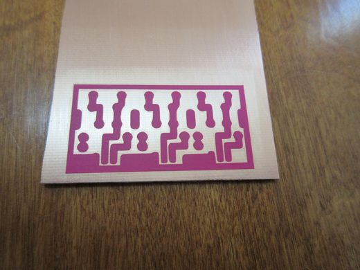
 Maybe a better design?
I made another circuit with a thicker trace pattern. The above picture shows the new pattern applied to the copper. The thicker traces and the larger outline should reduce the amount of copper removed during the etch (and reduce the etching time as well).
Hold the presses! Let’s try another approach!
 Hey, why not cut copper, not vinyl
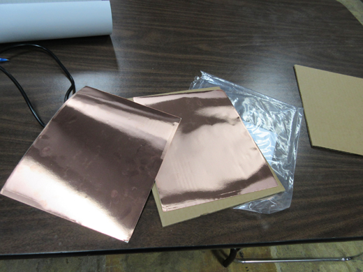
So my friend Lou suggested using some paper backed adhesive copper sheets to see how this would work. Instead of using a vinyl mask and dangerous chemicals to etch away copper, why not cut the copper and apply it to a substrate! Would the vinyl cutter work on this? Let’s give it a try!
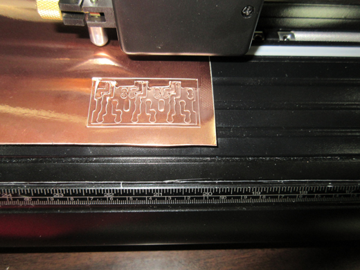
 First copper cut on this vinyl cutter
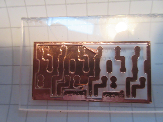
Using the “fat trace” pattern, the above picture shows the result of the cut. It’s not bad, but there appears to be some curling and lifting of the copper. Some adjustment will be needed to fix this problem. If I slow down the knife blade and greatly reduce the cutting depth I will get better results:

Weeding the copper while on the substrate
This is a bit of a welcome change compared to vinyl processing. Instead of weeding out copper on its adhesive backing, I simply removed the entire backing material from the copper foil and stuck in onto a substrate. In this case the substrate was a piece of clear plastic that I normally use for my intaglio printing project. The copper is then weeded out on the substrate; you get a home-made printed circuit without all the chemical mess!
 The holes, the holes!
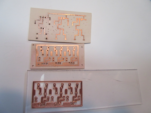
Some more manual steps are involved with all these circuits. The above picture shows three completed PCB’s. The top one is the acid etched thin line pattern. Drilling the holes in this one is possible, but not very easy. The fat traced pattern in the middle was easier for drilling holes and the acid etch process was faster. The bottom PCB was much easier to make and required no messy chemicals. My choice of substrate could have been better; while drilling the holes, the plastic material gummed up and pushed up some of the copper!
Next steps:
I will put components on these patterns and see if they work. I may make more of the acid etch boards because I have the materials, but I really like the adhesive copper foil approach better; It’s easier, faster, and it can be applied to a number of substrates. I just have to get better at drilling holes!
